In this post, we will quickly review the Configurable Logic Block (CLB) and how it has changed over the years.
In 1984, Xilinx introduced the first FPGA to the world, the XC2064. This FPGA formed the backbone of later device families and the design flow leveraged the Xilinx XACT tool.
Nearly 40 years later, FPGAs have come a long way. Devices are larger, faster, and more capable in a variety of ways. AMD (Xilinx) Vivado is a very polished, modern EDA tool leveraging universal HDLs in VHDL, Verilog, and System Verilog. Even so, some of the basic concepts have been around for a long time.
The Configurable Logic Block
The most important part of programmable logic designs is, as the name implies, the programmable logic elements. Programmable logic is arranged into groups called CLBs – Configurable Logic Blocks, small logic regions on the device.
While the XC2064 had 64 CLBs, in an 8×8 grid, many of the newest devices in the Versal family can have well over 100K CLBs. Not all CLBs are equal – Versal family CLBs are far more capable than older device families.
LUTs (Lookup Tables)
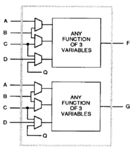
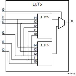
The first element of a Configurable Logic Block is the lookup table (LUT). These are logic functions of a varying number of inputs. The original LUT in the 2064 and the modern LUT6 used in recent architectures are compared below:


The LUT6 is far more versatile, since 5-input functions provide many more options than 3 input functions.
Flip Flops
The next element of a CLB is the flip flops. The flip flops are used for the synchronous logic that are the backbone of all FPGA designs. The flip flop design itself has not changed much – a flip flop is a flip flop – but the concentration of flip flops in CLBs has steadily increased. The table below shows the number of flip flops and LUTs per CLB in a few important generations.
| Device Family | Release Year | LUTS/CLB | FFs/CLB |
|---|---|---|---|
| XC2064 | 1984 | 1 LUT4 | 1 |
| Virtex | 1999 | 4 LUT4s | 4 |
| Virtex 5 | 2006 | 4 LUT6s | 4 |
| 7-Series/UltraScale/US+ | 2010/2013/2015 | 8* LUT6s | *16 |
| Versal | 2019 | 32 LUT6s | 64 |
As you can see, the number of resources per CLB keeps growing as the technology footprint shrinks. Note that there are significant differences between the 7-series and UltraScale CLBs despite a similar number of resources.
Multiplexer
Another key element of the CLB is the multiplexer. Multiplexers are used to select the output values of different inputs to create larger functions. LUTs perform the basic multiplexing and then the multiplexers can allow wider functions to be created.
Here’s an example for how a 6-input LUT could be used as a 4:1 multiplexer. The 5th and 6th inputs will act as the multiplexer selection bits, and based on those, the output will take on the value of a given input from I0-I3.
| I0 | I1 | I2 | I3 | I4 (S0) | I5 (S1) | O |
|---|---|---|---|---|---|---|
| D | X | X | X | 0 | 0 | D |
| X | D | X | X | 1 | 0 | D |
| X | X | D | X | 0 | 1 | D |
| X | X | X | D | 1 | 1 | D |
Wide MUXs
The problem here is, what if a function requires more than 4 inputs? That’s where the Wide MUXs come in. The F7 MUX combines 2 LUT multiplexers to create an 8:1 MUX. The F8 and F9 (when available) are used to create 16:1 and 32:1 MUXs by combining LUT outputs.
Carry Chains
The other resource in the CLBs are the carry chains (in newer families). Carry chains allow using the output of one LUT as the carry in of other LUTs without additional routing to connect the LUTs directly. The capacity of these carry chains has gradually increased from CARRY4s to CARRY8s to the new LOOKAHEAD8 in Versal devices.
Conclusion
This blog post went over the Configurable Logic Block, the backbone of all FPGA development. We discussed the resources in CLBs, how they are used in the bigger picture design, and how they have developed along with the technology over the years.
Some follow-up questions you might have are:
- How are CLBs routed to form full designs?
- What are some of the major configuration improvements to UltraScale CLBs and how do they make designs perform better?
- Moreover, how can I use this information to create higher-performance reliable designs?
If you’re interested in learning more, BLT’s Vivado Bootcamp 1 answers these questions and many more, in addition to covering the other types of resources available in FPGAs.