I/O timing constraints can be daunting, even for experienced FPGA designers. A common misconception is that these constraints somehow fix skewed input signals. They don’t. While synthesis and implementation tools can tolerate some signal misalignment, constraints are always required to determine whether your design will function correctly, as-is. If precise alignment is necessary, it must be handled manually using inserted primitives such as an IODELAY.
How Are I/O Timing Constraints Used?
I/O timing constraints communicate timing relationships between the FPGA and external devices, ensuring signals are captured and transmitted reliably. To define these constraints, you’ll typically need to refer to external component datasheets and understand your board’s physical characteristics.
Some designs might function without properly defined I/O timing constraints—often due to luck or overly conservative assumptions. But this is a fragile approach. Process variations, temperature shifts, and voltage fluctuations can all break a design that’s skating by without constraints. If reliability matters, defining accurate I/O timing is essential.
The Core Concepts Behind I/O Timing Constraints
The basic concepts are straightforward. For each signal crossing the FPGA boundary, constraints define a valid data window: the time during which a signal can be safely sampled or launched.
Input Constraints
set_input_delay -max: Maximum time from the clock edge to valid dataset_input_delay -min: Minimum time from the clock edge to valid data
Valid data window = Period – (Inmax – Inmin)
Output Constraints
set_output_delay -max: Setup time from clock edge to valid data at the receiving deviceset_output_delay -min: Hold time from clock edge to valid data at the receiving device
Valid data window = Outmax – Outmin

System Synchronous Clocking
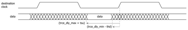
In system synchronous interfaces, both the FPGA and the external device use a shared or independent but synchronized clock. The FPGA receives or transmits data in sync with this external timing source.
When defining constraints for this scenario:
Input Constraints
set_input_delay -max= tclock-to-output max + ttrace delay maxset_input_delay -min= tclock-to-output min + ttrace delay min
These define the arrival window for valid data from the external device to the FPGA.
Output Constraints
set_output_delay -max= tsetup + ttrace delayset_output_delay -min= thold + ttrace delay
These ensure that data driven from the FPGA meets the setup and hold times at the receiving device.
Vendor-Specific I/O Timing Constraints Practices
AMD (Xilinx)
The AMD Vivado Design Suite utilizes Xilinx Design Constraints (XDC) files, which are based on the Synopsys Design Constraints (SDC) format. Key considerations include:
- I/O Planning: Vivado’s I/O Planning view allows designers to assign and validate I/O ports, ensuring compatibility with I/O standards and voltage requirements.
- Timing Constraints: Use
set_input_delayandset_output_delayto specify external delays. For example:
TCL
set_input_delay -clock clk -max 5.0 [get_ports data_in]
set_output_delay -clock clk -max 3.0 [get_ports data_out]
- I/O Delay Elements: AMD (Xilinx) FPGAs offer programmable I/O delay elements (e.g., IDELAY and ODELAY) to fine-tune timing.
- Timing Exceptions: Commands like
set_false_pathandset_multicycle_pathhelp manage complex timing scenarios.
Altera
Altera’s (Intel’s) Quartus Prime software also supports SDC-based constraints. Key aspects include:
- Timing Analyzer: This tool provides detailed reports on timing paths, highlighting any violations.
- Constraint Application: Use
set_input_delayandset_output_delayto define timing relationships. For instance:
TCL
set_input_delay -clock clk -max 6.0 [get_ports data_in]
set_output_delay -clock clk -max 4.0 [get_ports data_out]
- Report Generation: The
report_timingcommand generates comprehensive timing analysis reports.
Lattice Semiconductor
Lattice’s Radiant and Diamond design tools cater to their FPGA families. Notable features include:
- Programmable Delay Elements: Devices like the MachXO2 incorporate programmable delay cells to adjust input timing, aiding in meeting hold time requirements.
- Constraint Specification: Similar to other vendors, use
set_input_delayandset_output_delayto define timing constraints. - Timing Closure: Lattice emphasizes the importance of accurate constraints for achieving timing closure, especially when interfacing with high-speed peripherals.
Microchip
Microchip’s Libero SoC Design Suite provides a graphical interface for constraint management. Key points include:
- Constraint Dialogs: Users can specify input and output delays through dedicated dialog boxes, entering maximum and minimum values based on external timing budgets.
- Constraint Application: While the interface is GUI-based, the underlying principles align with SDC practices, ensuring consistency in timing analysis.
Attend Our Workshop on Timing Constraints

Do you struggle to identify which constraints are needed for a design or how to properly input them? This workshop will cover how to use features in Vivado, clock domain crossing strategies, and how to get the most out of static timing analysis for Versal devices.
Clock Uncertainty and Jitter with I/O Timing Constraints
I/O timing constraints assume an ideal clock edge, but real clocks are rarely perfect. Clock uncertainty accounts for jitter, phase noise, skew, and margin needed for safe operation.
In Vivado, Quartus, and other tools, you can specify for example 200ps of uncertainty with this command:
TCL
set_clock_uncertainty 0.2 [get_clocks clk]
This reduces the valid data window by subtracting uncertainty from both setup and hold margins. It’s especially important when interfacing with high-speed devices or using external clocks that may not be phase-aligned with internal clocks.
For best results:
- Refer to the jitter specifications in your clock source’s datasheet.
- Consider trace length mismatches between clock and data lines.
- For system-synchronous designs, budget for both source and destination clock uncertainty.
Multicycle and False Path Constraints
Not all timing paths are evaluated every cycle. Sometimes, data is allowed to arrive over multiple cycles (e.g., in handshake protocols), or the timing path isn’t relevant at all (e.g., asynchronous control signals). You need to tell the tool:
- Multicycle Paths:
- set_multicycle_path 2 -setup -from [get_ports data_in] -to [get_registers *]
This tells the tool that the signal only needs to be valid every 2 clock cycles.
- False Paths:
- set_false_path -from [get_ports async_flag]
This disables timing checks on paths where setup/hold analysis doesn’t apply.
Misusing or omitting these can either lead to unnecessary constraint violations or missed timing violations.
Conclusion
I/O timing constraints are pivotal for ensuring reliable FPGA operation, especially when interfacing with external components. While the fundamental principles remain consistent across vendors, each offers unique tools and features to aid in constraint specification and timing analysis. By understanding and leveraging these vendor-specific practices, designers can achieve robust and reliable FPGA designs.
