What is PCIe? PCI Express (PCIe) is a high-speed serial interface used to connect processors and peripherals in everything from servers and workstations to embedded systems and FPGAs. If your system needs to move a lot of data fast, it is likely the protocol that makes it happen.
PCI stands for Peripheral Component Interconnect in PCIe. It was the original parallel bus standard introduced in the 1990s for connecting peripherals like network cards and graphics cards to a motherboard. PCIe is its high-speed, serial successor that offers faster data transfer, improved scalability, and point-to-point connections.
But what exactly is PCIe, and what should embedded and FPGA engineers know to implement it effectively?
Point-to-Point Performance
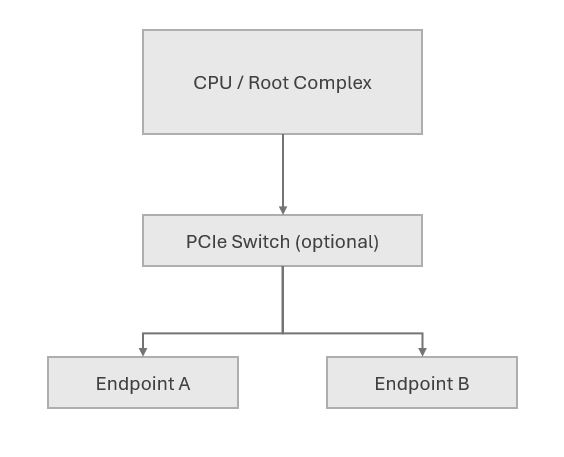
PCIe replaces older parallel bus architectures with a scalable, point-to-point serial interface. Each PCIe link connects exactly two devices, a Root Complex (usually a CPU or host) and an Endpoint (such as a network card, SSD, or FPGA).
Each link consists of lanes: full-duplex differential pairs that carry data simultaneously in both directions. The number of lanes is denoted by “x1”, “x4”, “x8”, “x16” or “x32”.
Link Diagram

Each connection supports high-throughput, low-latency transactions without bus contention.
PCIe Generations and Bandwidth
PCIe has evolved over multiple generations. Each jump increases the raw transfer rate per lane:
| Generation | Transfer Rate (GT/s) | Encoding | Effective Throughput per Lane | x1 Bandwidth | x16 Bandwidth |
|---|---|---|---|---|---|
| Gen1 | 2.5 GT/s | 8b/10b | ~250 MB/s | 250 MB/s | 4 GB/s |
| Gen2 | 5.0 GT/s | 8b/10b | ~500 MB/s | 500 MB/s | 8 GB/s |
| Gen3 | 8.0 GT/s | 128b/130b | ~1 GB/s | 1 GB/s | 16 GB/s |
| Gen4 | 16.0 GT/s | 128b/130b | ~2 GB/s | 2 GB/s | 32 GB/s |
| Gen5 | 32.0 GT/s | 128b/130b | ~4 GB/s | 4 GB/s | 64 GB/s |
The protocol is backward compatible, meaning a Gen4 device will operate in a Gen3 slot at Gen3 speeds.
Key Concepts for FPGA and Embedded Engineers
- Root Complex (RC): Initiates PCIe transactions, usually a processor or host.
- Endpoint (EP): Responds to transactions, typically a peripheral or FPGA.
- TLP (Transaction Layer Packet): The data format used in PCIe communication.
- BAR (Base Address Register): A register in the Endpoint that tells the host where to map the device’s memory space.
- AXI4-PCIe Bridge: Common interface inside SoCs and FPGAs to convert internal AXI bus traffic to PCIe-compliant packets.
- DMA (Direct Memory Access): Used to transfer large amounts of data without processor intervention.
Example: Setup in AMD Vivado
Let’s say we want to implement a PCIe Endpoint on an AMD (Xilinx) FPGA:
Step 1: Instantiate PCIe IP
In Vivado, instantiate the “XDMA PCIe” IP core:
- Select number of lanes (e.g., x4)
- Choose PCIe Gen3
- Enable AXI Memory-Mapped (AXI-MM) and/or Streaming (AXI-S) interfaces
- Enable DMA if needed
Step 2: Connect AXI Interfaces
Use Vivado block design to connect:
- AXI Master from PCIe IP to on-chip memory or external DDR
- AXI-Lite for configuration registers
Step 3: Apply Constraints
Example .xdc constraints for PCIe lanes:
TCL
set_property PACKAGE_PIN R12 [get_ports pcie_txp[0]]

set_property IOSTANDARD DIFF_SSTL12 [get_ports pcie_txp[0]]

# Repeat for all TX/RX pairs
Also include timing constraints and clocking assignments based on the board’s reference clock.
Step 4: BAR Configuration
Set BARs to expose specific regions of FPGA memory to the host:
TCL (pseudocode)
BAR0: 64-bit Memory, 256 KB

BAR1: 32-bit Memory, 128 KB
These regions can then be mapped by the host OS driver.
Example: Basic PCIe TLP Format (Memory Write)
[Header (3 DW)] [Data Payload]

└─> Includes address, length, and type (e.g., MemWr)
The Root Complex issues a MemWr to the Endpoint’s BAR-mapped address, and the PCIe IP on the FPGA decodes it into AXI transactions.
Troubleshooting Tips
- Link not training? Check reference clock, lane polarity, reset signals.
- Unexpected BAR behavior? Confirm enumeration and size settings.
- DMA hangs? Validate descriptor queues and interrupt logic.
- Timing failures? Look for AXI clock domain crossings and high fan-out paths in synthesis.
PCIe Design Best Practices Checklist
Reset & Link Training
- Assert and release PERST_N correctly during system reset.
- Ensure proper reference clock source (usually 100 MHz differential).
- Confirm link training status (LTSSM) via debug or ILA.
IP Core Configuration
- Match PCIe generation and lane width to board specs.
- Enable only necessary features (e.g., BARs, DMA, interrupts).
- Set BAR sizes carefully—must match host driver expectations.
Constraints & Timing
- Use proper XDC constraints for differential pairs and clocks.
- Check for false paths and crossing clock domains.
- Run full implementation timing analysis—even for x1 designs.
AXI & DMA Integration
- Verify AXI clock domain matches rest of system or bridge cleanly.
- Implement and test proper DMA descriptors and buffer handling.
- Handle backpressure correctly on streaming AXI interfaces.
Interrupts & Status
- Use MSI or MSI-X for signaling events to the host.
- Map and acknowledge interrupts in both FPGA and host software.
- Monitor PCIe status and error signals (e.g., cfg_err_*).
Host Interaction
- Test with lspci, setpci, and memory-mapped reads/writes.
- Verify correct enumeration and device IDs.
- Handle unexpected or out-of-order host accesses gracefully.
Debug & Bring-Up
- Use ILA to monitor AXI and PCIe status signals.
- Enable PCIe debug ports (e.g., LTSSM state, received TLPs).
- Log all DMA or TLP activity during early bring-up.
Conclusion
PCIe is a core interface for connecting high-speed components in embedded systems. Its scalable architecture, packet-based communication, and DMA support make it suitable for applications including storage, networking, and FPGA-based accelerators. A solid understanding of PCIe from physical signaling and protocol layers to memory mapping and data transfer is essential for building efficient designs. As systems grow more complex, careful attention to PCIe configuration, integration, and validation becomes increasingly important.


