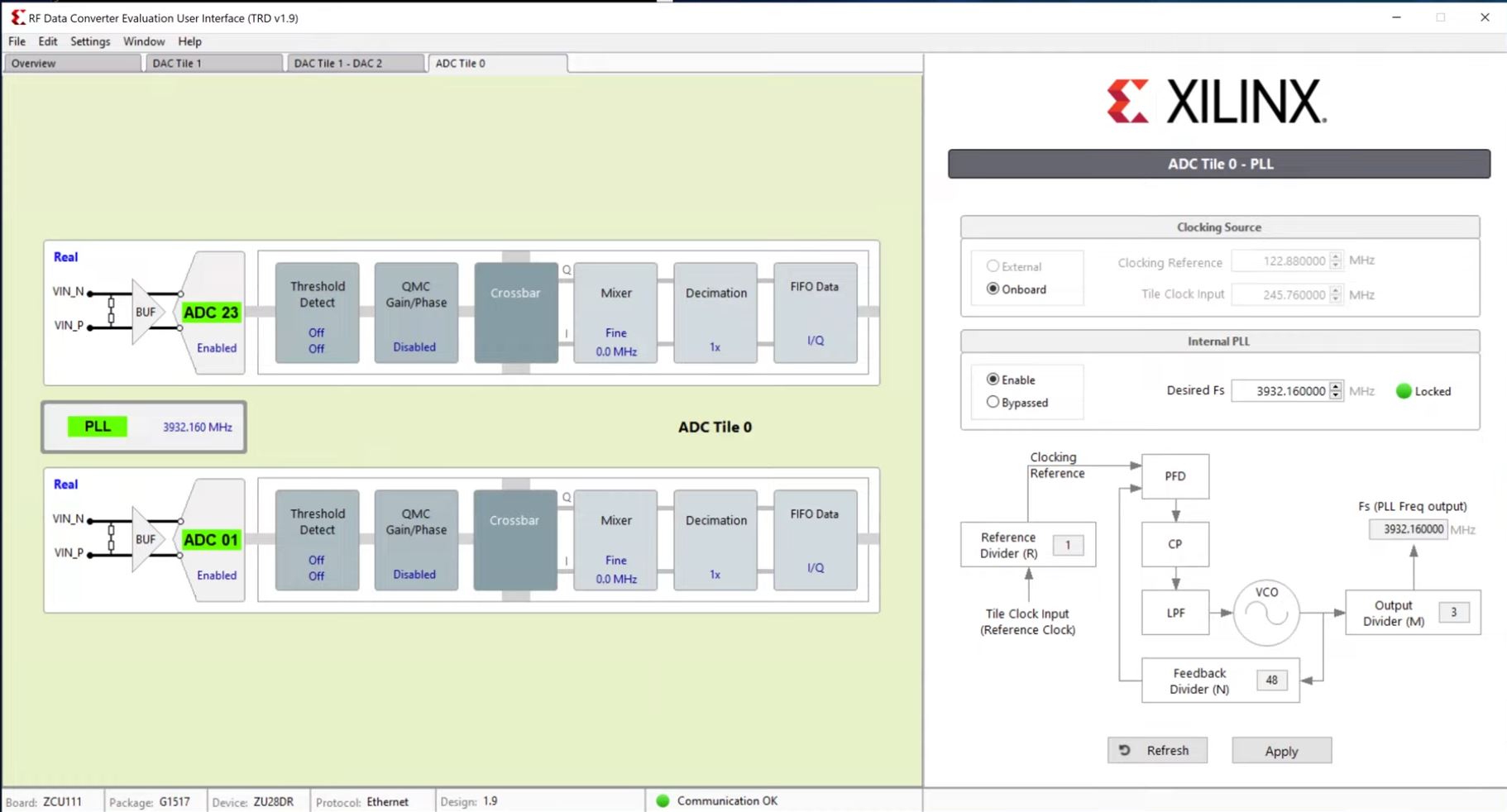
The RF Analyzer in AMD Vivado represents a significant advancement in RF signal processing and analysis, tailored to address the complex requirements of modern communication systems, radar applications, and more. By bridging sophisticated configuration capabilities with user-friendly GUI controls, the tool equips engineers with the precision and flexibility required for optimal ADC (Analog-to-Digital Converter) and DAC (Digital-to-Analog Converter) performance.
This comprehensive platform reduces the barriers to entry for RF system design, providing a seamless way to configure, analyze, and test RF signals. By supporting most API functions and configuration options for ADCs and DACs, the RF Analyzer becomes a crucial asset in streamlining the design and testing phases of RF signal processing workflows.
Key Features and Functionalities of the RF Analyzer
For a detailed breakdown of these features, refer to the AMD official user guide, UG1309: RF Data Converter Interface, which provides in-depth explanations and step-by-step instructions for configuring and utilizing the RF Analyzer effectively.
Versatile RF Analyzer Configuration Options
The RF Analyzer offers a wide range of configuration options that are essential for fine-tuning ADC and DAC operations. The GUI’s intuitive interface makes it possible to adjust clock, power, and crossbar settings effortlessly. These configurations are critical for adapting to various signal formats and operational scenarios.
- Clock Settings: Engineers can configure external PLLs to predefined frequencies with ease. Synchronization through the LMK clock source ensures precise clock alignment, a key factor in achieving coherent sampling and signal integrity.
- Power Settings: Adjusting DAC drive modes allows fine control over output signal power. Engineers can configure milliamp levels for precision output, ensuring optimal performance in sensitive RF applications.
- Crossbar Functionalities: Whether the signal format is real or complex (IQ), the crossbar provides tailored modes for different signal placements relative to the sampling frequency. This adaptability is critical for systems that require specific signal modulation and demodulation strategies.
ADC and DAC Configuration
The tool’s ability to fine-tune ADC and DAC settings is one of its standout features. By enabling detailed adjustments, engineers can optimize their systems for performance, efficiency, and signal quality.
- ADC Settings: The ADC configuration interface supports operational adjustments such as multiband processing and complex signal handling. With precise sampling frequency alignment, ADCs ensure accurate demodulation, preserving signal fidelity.
- DAC Settings: DAC configurations include advanced features such as low noise mode, enhanced linearity, and mix mode operations within the Nyquist zone. Additionally, clock generation and digital up-converter (DUC) functionalities, such as NCO frequency and interpolation rate adjustments, are seamlessly integrated.

Advanced Analysis and Sampling Support
The RF Analyzer extends its utility with robust sampling and analysis support. Engineers can simultaneously generate and capture samples in real and complex modes for FFT (Fast Fourier Transform) analysis. This capability is particularly valuable in characterizing signal integrity, identifying harmonic distortions, and ensuring the system meets stringent RF performance requirements.
Coherent sampling is achieved through precise synchronization of DAC and ADC clocks. Whether using on-chip PLLs or external sources, this synchronization minimizes phase noise and jitter, ensuring accurate signal representation. Additionally, the test environment allows for generating an integer number of complete samples, reducing windowing effects and enhancing FFT calculation accuracy.
Practical Demonstration Workflow
The RF Analyzer supports a structured workflow for testing and analyzing RF systems. This workflow demonstrates how the tool integrates into engineering processes to achieve precise signal generation and evaluation.
Initial Setup for the RF Analyzer
Setting up the tool involves straightforward steps to ensure the evaluation environment is ready:
- Power on the Evaluation Board and configure the LMK clock settings for synchronization.
- Launch the GUI application and initialize the system, ensuring all components are recognized and ready.
- Access the overview tab in the GUI to review and configure system clock and power settings, tailoring the setup to specific testing requirements.
- Press Submit.
- Verify the PLL lock status and ensure correct sampling rate synchronization before proceeding with signal generation.
Signal Generation and Analysis
- Single-Tone Signal Generation: Engineers can configure DAC tiles for specific sampling frequencies and real single-band operations. These settings are validated through oscilloscope measurements, ensuring the generated signals meet expected criteria for amplitude, phase, and frequency.
- Multi-Tone and Complex Modulation: The tool provides options for generating complex waveforms, such as multi-tone and QAM-modulated signals, to simulate real-world RF scenarios.
- Two-Tone Signal Analysis: Extending configurations to dual-tone signals allows for more complex testing scenarios. By analyzing the FFT output, engineers can identify harmonic distortions, intermodulation products, and spurs, ensuring compliance with system specifications.
ADC Capture and Evaluation
ADC testing involves capturing input signals and performing detailed analysis:
- Signal Acquisition: Engineers can set ADC sampling frequencies and align crossbar settings with DAC configurations to ensure coherence.
- Time and Frequency Domain Analysis: The GUI provides real-time visualization tools for monitoring captured waveforms, spectrum analysis, and power levels.
- Data Analysis: Using FFT and other analysis tools, engineers can measure critical parameters such as harmonic distortion, signal-to-noise ratio (SNR), and spurious-free dynamic range (SFDR).
This workflow highlights the tool’s ability to streamline testing processes while delivering precise and actionable insights.
Enhanced Applications and Benefits of the RF Analyzer
The RF Analyzer is not just a testing platform; it is a solution that drives innovation in RF system design. Its applications span across multiple industries:
- Communication Systems: Optimize signal paths for 5G networks, ensuring high-speed data transfer with minimal distortion.
- Radar Systems: Fine-tune ADC and DAC configurations to achieve superior resolution and range in radar applications.
- IoT and Embedded Systems: Support lightweight, high-performance designs tailored for connected devices.
By integrating advanced features with robust hardware support, the tool simplifies RF system design and testing. Its intuitive interface ensures that even complex configurations are accessible, empowering engineers to achieve their design goals efficiently.
Conclusion
The RF Analyzer exemplifies the power of combining advanced RF technology with user-friendly interfaces. Its comprehensive features, seamless hardware integration, and structured workflows make it an invaluable resource for RF engineers. Whether it’s designing cutting-edge communication systems, refining radar performance, or optimizing IoT devices, this tool enhances every aspect of RF signal processing and analysis.
Additionally, the RF Analyzer aligns with AMD’s broader tool ecosystem, providing compatibility with other AMD development and debugging tools to create a more cohesive and efficient RF design workflow.


